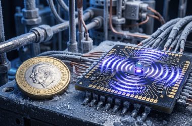
At 10 millikelvin, roughly 273 degrees below zero, a transistor in a University of Hong Kong lab is doing something unexpected. It fires electrical spikes not continuously or randomly, but in the precise pattern of a biological neuron. The chip is not malfunctioning. That is the point.
The team behind this result, led by Professor Yuhao Zhang and PhD student Xin Yang at HKU’s Department of Electrical and Computer Engineering, set out to build a cryogenic neuromorphic chip that could operate within a quantum computer without generating the heat that currently prevents such integration. What they found along the way was stranger and more useful than they expected.
Quantum computers are extraordinarily sensitive machines. Their qubits, the fundamental units of quantum information, must be kept at millikelvin temperatures to preserve fragile quantum states. The problem is silicon-based electronics controlling those qubits cannot operate near that cold without consuming significant power and releasing heat. Engineers place control electronics far from the qubits, connecting them with long, tangled wiring. As quantum processors grow, that wiring becomes a serious bottleneck. You cannot build a machine with thousands of qubits if each needs its own cable running back to a warm room.
Zhang and Yang worked with Silicon Carbide MOSFETs, a type of transistor common in electric vehicle power systems and industrial grids. SiC is a rugged, well-understood material, and the researchers used industry-standard devices rather than laboratory curiosities. Cooling those devices below 2 kelvin produced results not predicted by standard semiconductor theory.
The transistors began exhibiting what physicists call negative differential resistance, specifically an S-shaped current-voltage curve. In most devices, current increases as voltage increases. In these cooled SiC transistors, raising the voltage beyond a certain threshold caused the current to drop sharply before rising again, tracing a distinctive S-shaped curve on the graph. The mechanism driving this is electron-donor impact ionisation (EDII): free electrons at cryogenic temperatures gain enough energy to knock loosely bound electrons from donor atoms in the crystal lattice, producing an avalanche effect that triggers the sharp switching behaviour. The effect arises from the material’s atomic structure, not from thermal processes, so it remains stable and repeatable across different manufacturing batches.
That S-shaped curve is exactly what you need to reproduce the spiking behaviour of a biological neuron. In neuroscience, the Hodgkin-Huxley model describes how nerve cells fire: below a threshold, nothing happens; above it, the cell fires a sharp electrical pulse and then resets. The SiC transistor, cooled to 10 millikelvin, does the same thing with a single device. No additional circuitry. No external triggers. One transistor, behaving like a nerve cell.
The energy efficiency numbers are striking. The cryogenic neuromorphic chip consumes thousands of times less power than conventional cryogenic electronics performing equivalent functions. That difference matters enormously when the goal is to place control electronics directly alongside qubits without heating them. “By using the unique carrier dynamics in silicon carbide, we can create circuits that are thousands of times more energy-efficient than conventional electronics, significantly reducing the thermal load on cryogenic systems,” Professor Zhang said in a statement accompanying the paper.
A single artificial neuron is an interesting result. A network of them is potentially useful. Zhang’s group demonstrated that their SiC-based neurons can be cascaded, connected in series so that the output spike from one device triggers the next. That cascading behaviour is the foundation of any neuromorphic computing system, and it brings the technology a step closer to performing real operations: quantum error correction, real-time qubit monitoring, or pattern recognition inside the cryostat itself.
The manufacturing angle matters too. SiC is not an exotic research material. It is produced on 300-millimetre wafers at industrial foundries worldwide. That means the path from laboratory demonstration to scaled production does not require building new factories or developing new processes from scratch. The HKU team’s findings, published in Nature Communications, used devices from facilities of exactly the kind already supplying the EV industry.
Deep-space exploration is a potential application alongside quantum computing. Spacecraft venturing to the outer solar system, or instruments left on the lunar surface, face ambient temperatures not far above absolute zero. Electronics that work reliably at millikelvin temperatures without demanding a power-hungry heater to keep them warm could prove valuable in those environments, too.
Engineering Deep Dive: How SiC Transistors Mimic Neurons at Millikelvin Temperatures
To understand why the University of Hong Kong’s result is significant, it helps to understand what a neuron actually does and why reproducing that behaviour in silicon has proved so difficult at room temperature, let alone near absolute zero.
A biological neuron maintains a resting potential of roughly minus 70 millivolts across its membrane. When incoming signals push that potential above a threshold of around minus 55 millivolts, ion channels snap open, sodium ions flood in, and the membrane potential shoots to plus 40 millivolts in about a millisecond before potassium channels pull it back down. That all-or-nothing response is called an action potential. The neuron then enters a brief refractory period before it can fire again. The energy cost is tiny, around 10 femtojoules per spike, and the temporal precision is striking.
Neuromorphic engineers have spent decades trying to replicate this behaviour in silicon because conventional computing architectures, in which data and processing are physically separate, and information is encoded as binary 0s and 1s, are fundamentally inefficient for tasks the brain handles effortlessly, such as pattern recognition, sensory processing, and adaptive learning. Brain-inspired chips promise to do those tasks with far lower energy consumption by encoding information in spike timing rather than voltage levels.
Most existing neuromorphic platforms, such as Intel’s Loihi chip or IBM’s TrueNorth, operate at room temperature and use multiple transistors wired together to approximate the threshold-and-spike behaviour of a neuron. They work, but the circuit complexity is significant. The HKU approach is different: a single SiC MOSFET, properly cooled, exhibits the necessary non-linear switching behaviour on its own.
The physics behind this is worth unpacking. A MOSFET (Metal-Oxide-Semiconductor Field-Effect Transistor) works by using a gate voltage to control the flow of charge carriers, electrons or holes, through a semiconductor channel. In standard silicon at room temperature, the relationship between gate voltage and drain current is well-behaved and monotonic: more gate voltage means more current. At cryogenic temperatures, however, the thermal energy available to charge carriers drops dramatically. In silicon carbide, which has a wider bandgap than silicon (3.26 electron volts versus 1.12 eV for silicon), donor atoms that readily release electrons at room temperature hold on to them much more tightly when cooled. Those electrons become “frozen out”, trapped on their donor sites.
As voltage rises past a critical point, those trapped electrons gain enough kinetic energy to ionise neighbouring donor atoms through impact, releasing a cascade of free carriers. This is electron-donor impact ionisation (EDII). The sudden availability of extra carriers causes the current to jump sharply before the device’s own internal feedback pulls it back, producing the S-shaped negative differential resistance curve. The S-shape is the key: it means the device has two stable states at a given voltage, a low-current state and a high-current state, with an unstable region between them. That bistability is precisely what generates the threshold-and-spike behaviour.
The wide bandgap of SiC is what makes this effect so clean and reproducible. In narrow-bandgap materials, the donor freeze-out is less complete, and the EDII cascade is less sharp. SiC’s bandgap is large enough that the transition from frozen to ionised carriers is abrupt, giving a well-defined threshold, which maps directly onto the all-or-nothing firing of a biological neuron.
From a circuit design perspective, a single-transistor neuron is highly attractive. It reduces component count, which reduces both the physical footprint on a chip and the power dissipated per neuron. When you are trying to place thousands of these neurons inside a dilution refrigerator alongside a quantum processor, every microwatt matters. The HKU team measured their devices operating with power consumption in the nanowatt range, several orders of magnitude below the microwatt budgets of conventional cryogenic CMOS circuits.
The cascading demonstration is equally important from an engineering standpoint. For a neuromorphic system to be useful, neurons must communicate: the output spike of one neuron must be capable of driving the input of the next. Zhang’s group showed that their SiC neurons can be connected in this way without loss of signal integrity at 10 millikelvin. That is a non-trivial result, because at cryogenic temperatures parasitic capacitances and resistances in interconnects behave differently than room-temperature models predict, and signal propagation can degrade unexpectedly.
The manufacturing readiness is another dimension worth examining. SiC device fabrication has matured enormously over the past decade, driven largely by demand from the electric vehicle industry for high-power, high-efficiency inverters. SiC MOSFETs are now produced on 150-millimetre and 300-millimetre wafers at fabs in Europe, the United States, and Asia. The HKU researchers used commercially available devices, which means their characterisation of the EDII effect reflects what you would actually get from production-line hardware, not specially grown research samples. That reproducibility across batches, which the team confirmed, is what makes the technology credible as a scalable platform rather than a laboratory curiosity.
The paper, published in Nature Communications and co-authored by Xin Yang, Matthew Porter, Yuan Qin, and colleagues, points toward quantum error correction as the most immediate application. Current error correction schemes require classical processors to monitor qubit states and apply corrections in real time. Moving that processing into the cryostat, using a cryogenic neuromorphic chip operating at the same temperature as the qubits, would dramatically reduce the latency and wiring complexity that currently limit how quickly corrections can be applied. Whether SiC-based neuromorphic circuits are fast enough and flexible enough for that role is the next question the field will need to answer.
What Professor Zhang’s group has demonstrated is that the extreme cold of a quantum computer’s operating environment need not be a barrier to placing intelligent, energy-efficient electronics right where they are needed. Silicon carbide, a material already trusted to handle tens of kilowatts in electric cars, turns out to have a hidden talent at temperatures colder than deep space. The gap between today’s cumbersome quantum control systems and a compact, integrated quantum processor just got measurably smaller.
- University of Hong Kong engineers made a single transistor mimic brain-cell spiking at temperatures near absolute zero
- The chip uses silicon carbide MOSFETs that exhibit unusual negative differential resistance when cooled below 2 kelvin
- It is thousands of times more energy-efficient than conventional cryogenic electronics, reducing heat near quantum processors
- SiC is already mass-produced for electric vehicles, so manufacturing can scale using existing foundries