
Energy & Environment
EPFL and CSEM researchers achieve a certified 30.02% efficiency with a perovskite-silicon triple-junction solar cell, beating the previous 27.1% record.
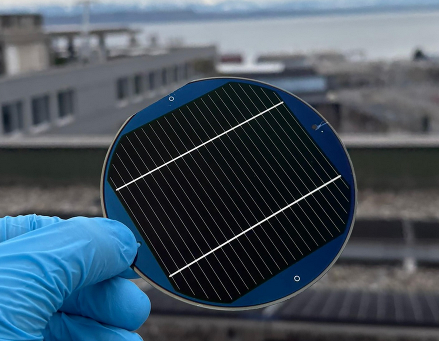
• Researchers at EPFL and CSEM have achieved a certified 30.02% efficiency with a perovskite-silicon triple-junction solar cell, smashing the previous 27.1% record.
• The device stacks two perovskite layers on silicon, with each layer capturing a different part of the solar spectrum.
• Three innovations enabled the leap: a defect-reducing molecule, a three-step fabrication process, and nanoparticle light-trapping between layers.
• Triple-junction cells have a theoretical efficiency limit above 40%, and perovskites could eventually rival space-grade cells at a fraction of the cost.
In 2018, a research team in Switzerland stacked three semiconductor layers on top of one another and pointed them at the sun. Their prototype solar cell converted 13% of the incoming light into electricity.
That number was respectable for a first attempt, but hardly threatening to the silicon panels already bolted to rooftops worldwide. Eight years later, the same laboratory has pushed the figure to 30.02%, independently certified and published in Nature. The jump matters, not because 30% is a round number, but because it puts a relatively cheap technology within striking distance of the ultra-expensive cells used on satellites.
The device was built at EPFL and CSEM, two Swiss research institutions with a long track record in photovoltaics. It is a triple-junction cell, meaning it contains three light-absorbing layers, each tuned to capture a different slice of the solar spectrum. The bottom layer is conventional silicon, which handles red and near-infrared light efficiently. On top sit two thin films of perovskite, a class of crystalline materials that can be deposited cheaply from solution and tuned to absorb specific wavelengths by adjusting their chemical composition. One perovskite layer targets the middle of the spectrum. The other captures higher-energy blue and ultraviolet photons. Between them, the three layers harvest a broader swathe of sunlight than any single material can manage alone.
The previous certified record for this type of cell stood at 27.1%. Closing a three-percentage-point gap demanded solutions to three distinct engineering problems. First, the top perovskite layer needed to produce a higher voltage. The team introduced a molecule that guides perovskite crystal formation during deposition, eliminating atomic-scale defects that trap charge carriers and waste energy. With fewer defects, the top cell now generates 1.4 volts under illumination, a substantial increase.
Second, the middle perovskite layer needed to absorb more near-infrared light. The researchers developed a three-step fabrication process, building the film in stages rather than in a single deposition, that improved the crystal structure and pushed the absorption edge deeper into the infrared. Third, light that passed through the middle layer without being absorbed needed to be redirected back in. The team positioned nanoparticles between the middle and bottom cells that scatter unabsorbed photons back into the perovskite, giving it a second chance to convert them.
Christophe Ballif, who leads the photovoltaics research at EPFL, has pointed out that triple-junction cells have theoretical efficiency limits well above 40%, meaning there is considerable headroom above the current record. The comparison with space-grade solar cells is instructive. Cells based on III-V semiconductors, the type used on the International Space Station and in satellite arrays, achieve around 37% efficiency but cost roughly a thousand times more per watt to manufacture. Perovskite layers can be deposited from liquid solutions at low temperatures, a process far closer to printing than to the high-vacuum epitaxy required for III-V cells. If the durability problems that have historically dogged perovskites can be solved, the cost advantage could be transformative.
Lead researcher Kerem Artuk and the wider team are now focused on scaling the technology from the current 54 cm² test cell to modules large enough for commercial production. The challenge is maintaining uniformity across larger areas: perovskite films deposited over tens of centimetres tend to develop variations in thickness and composition that reduce performance. Solving this is an engineering problem, not a physics one, which is often a good sign for eventual commercialisation.
Engineering deep dive
A standard silicon solar cell wastes most of the sunlight that hits it. A-level Physics students learn that a photon must have energy equal to or greater than the semiconductor's band gap to generate an electron-hole pair. For silicon, the band gap is about 1.1 electron volts (eV). Photons with less energy pass straight through. Photons with more energy do generate charge carriers, but the excess energy above 1.1 eV is lost as heat. This thermalisation loss is the single biggest reason why a silicon cell cannot exceed about 29% efficiency, no matter how perfectly it is made. The Shockley-Queisser limit, a calculation from 1961 that A-level students may encounter in extension material, puts the theoretical maximum for a single-junction cell at 33.7%.
A multi-junction cell sidesteps this problem by stacking materials with different band gaps. The top layer has a wide band gap and absorbs high-energy photons efficiently, generating a high voltage per photon. Lower-energy photons pass through to the next layer, which has a narrower band gap suited to absorbing them. In a triple-junction device, three layers divide the spectrum into three portions, each captured near its optimal voltage. The theoretical efficiency limit for a triple-junction cell under normal sunlight is around 49%, far above the single-junction ceiling.
Perovskites are attractive for multi-junction cells because their band gap is tuneable. The general crystal structure is ABX₃, where A is typically a large organic cation (such as methylammonium or formamidinium), B is a metal (usually lead), and X is a halide (iodine, bromine, or chlorine). By varying the ratio of halides, researchers can shift the band gap continuously from about 1.2 eV to over 2.3 eV. This tunability is unusual among semiconductors and makes perovskites ideal partners for silicon in tandem and triple-junction architectures.
The three-step fabrication process for the middle cell is an example of engineering meeting chemistry. Perovskite films are typically deposited by spin-coating a precursor solution onto a substrate and then heating it to crystallise the film. The problem is that a single-step process tends to produce crystals with random orientations and numerous grain boundaries, which act as sites where charge carriers recombine and are lost. By depositing the precursor in three stages, with controlled drying and annealing between each, the team encourages the crystals to grow in a preferred orientation with fewer grain boundaries. The result is a more ordered film that conducts charge more efficiently.
The nanoparticle interlayer between the middle and bottom cells works on a principle familiar from A-level optics: scattering. Photons that pass through the middle perovskite layer without being absorbed hit the nanoparticles and are scattered at wide angles. Many of these scattered photons re-enter the perovskite layer from below, effectively doubling its optical thickness without increasing its physical thickness. This is a form of light trapping, a technique widely used in silicon cell design but here adapted for the internal interface of a multi-junction stack.
For students interested in the maths, the current matching condition is worth understanding. In a series-connected multi-junction cell, the total current is limited by the layer producing the least current. This means the band gaps and thicknesses of all three layers must be carefully balanced so that each generates roughly the same photocurrent. Getting this wrong, even slightly, means one layer becomes a bottleneck. The optimisation is a multi-variable problem that links material composition, film thickness, and optical design, exactly the kind of challenge that makes photovoltaic engineering a rich field for applied physics graduates.
The 30% milestone is a waypoint, not a destination. The theoretical headroom remains substantial, and the cost structure of perovskite deposition favours mass production. Whether these laboratory results can survive the jump to factory-scale manufacturing, and whether perovskite cells can match silicon's 25-year outdoor durability, remain open questions. But the trajectory since 2018, from 13% to 30% in eight years, suggests that the answers may arrive sooner than the sceptics expect.
Links to the curriculum: A level
Credit via pv-magazine.com
Energy & Environment

Electronics & Communications
Energy & EnvironmentBreakthroughs

Construction & Infrastructure