
Electronics & CommunicationsBreakthroughs
An atomically thin transistor breakthrough from NYCU and TSMC uses a 0.42nm interface layer to push chip performance beyond today's silicon limits.
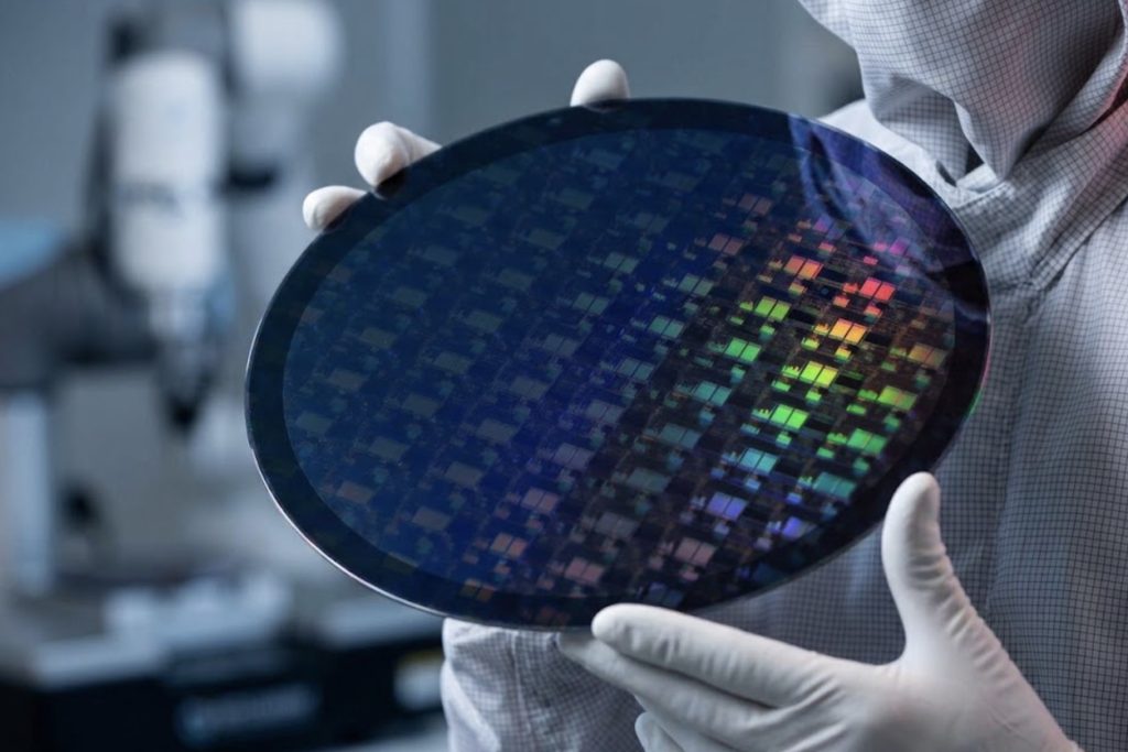
The way chip makers have managed to overcome the limitations of shrinking silicon involves a single interface that is just 0.42 nanometres thick. Scientists at National Yang Ming Chiao Tung University (NYCU) in Taiwan, in collaboration with TSMC Corporate Research, have developed what appears to be a real breakthrough in atomically thin transistors: a layer that has been built atom by atom and which resolves the compromise that has long plagued two-dimensional chip research.
The problem that the team wanted to solve has been part of research into 2D semiconductors for years. Monolayer molybdenum disulphide, or MoS2, is a single layer of atoms which acts as a semiconductor and is usually regarded as one of silicon’s most promising replacements. Using thinner gate dielectrics on top of that layer allows engineers to have better control over the transistor’s switching behaviour, but when an ultrathin dielectric is deposited directly onto the MoS2 the surface tends to be rough and full of defects, causing the electrons moving through the channel below to be scattered and thus reducing performance. The more control you improve, the more you damage the electron flow that you are trying to control.
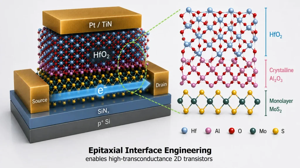
The solution put forward by the team from NYCU and TSMC, which appeared in Nature Electronics, was to cease viewing the interface as a secondary concern and to design it directly. They produced a sheet of monolayer MoS2 by means of chemical vapour deposition (CVD), a technique which is much easier to scale up for use in wafer production than the method of adding flakes one by one that is typical in current 2D materials research. On this sheet they then applied an extremely thin layer of epitaxial aluminium, so that the aluminium atoms arrange themselves in a crystalline structure that corresponds to the MoS2 below. Oxidising this aluminium layer yielded approximately 0.42 nanometres of aluminium oxide, after which a layer of hafnium oxide - a dielectric that is already used in commercial chips - was placed on top.
The thin buffer carries out two functions: it provides the hafnium oxide with a smooth and even surface on which to grow, as opposed to the rough native surface of bare MoS2, and it gives physical protection to the semiconductor’s electrons against the defects and dangling bonds that would otherwise appear at the interface due to the poor match between the two materials. Transistors constructed using this structure had a transconductance of 0.45 milliSiemens per micrometre in channels about 100 nanometres long, a value indicating how effectively the transistor’s gate voltage can control the flow of current, a result that is comparable to that of much more established technologies.
It is important to use MoS2 that has been grown by CVD rather than that which has been peeled from a bulk crystal since this relates to how such transistors might one day be manufactured. Although exfoliated flakes are useful for demonstrating that a concept works, no factory could possibly produce billions of chips by removing the flakes one at a time from crystals. A method that is compatible with CVD growth and involves standard procedures such as oxidation and atomic layer deposition is one that a factory like TSMC’s could plausibly bring into industrial production, which is exactly why the company’s own research division co-authored the study.
Engineering deep dive
At its core, every transistor is a switch that is controlled by voltage and not by a mechanical lever. In a field-effect transistor, which is the type used in almost every modern chip, a voltage applied to the gate electrode produces an electric field that either permits or obstructs the current flowing between two other terminals, the source and the drain, via a channel made of semiconducting material. Located between the gate electrode and the channel is the gate dielectric, an insulating layer which allows the electric field to pass through while preventing any current from leaking across it. A-level physics students will be familiar with this basic principle from their study of capacitors: the gate, the dielectric and the channel make up a structure very similar to a parallel-plate capacitor, and the thinner the dielectric, the greater the electric field it can produce for a given voltage, which is the reason why engineers have been spending decades attempting to make it thinner.
It is precisely because capacitance increases as the dielectric becomes thinner that reducing the thickness of this layer has always been such an aim, and it is also precisely for this reason that problems eventually arise. If you try to reduce the dielectric to just a few atoms in thickness two issues begin to oppose you. On the one hand, the electrons can start to tunnel directly through it as a result of quantum mechanical tunnelling, causing current to leak even when the transistor is supposed to be off and thus wasting power. On the other hand, and this is exactly what the NYCU and TSMC team focused on, the physical process of depositing a layer that thin tends to leave a rough and defect-filled interface with the material below it, and the defects at this interface scatter the electrons moving through the semiconductor channel, lowering what engineers refer to as carrier mobility.
Chip designers find monolayer MoS2 of interest since it has no dangling bonds on its surface, the surface consisting of a single layer of atoms with nothing projecting out to react in an unpredictable way with any material that is deposited on top. In principle, this should make it easier to grow a dielectric on than on silicon. In practice, however, most dielectric deposition methods still result in a rough and poorly matched interface when used directly on 2D materials, since the growth chemistry developed for silicon does not transfer smoothly. The mismatch is the exact trade-off that this research deals with: by using an epitaxial aluminium layer, with its atomic structure aligned with that of the MoS2 crystal lattice below it, the subsequent oxide layers are given a surface on which to grow cleanly, rather than nucleating at random over a rough surface.
Anyone who is studying electronics should understand transconductance, the criterion the group used to evaluate their devices. It is a measure of how much the drain current varies for a particular change in gate voltage, that is to say, how sensitively the switch reacts to its control signal. The greater the transconductance, the faster the transistor can switch and the more current it can deliver for the same variation in gate voltage, both of which are important when constructing fast and energy-efficient logic circuits. Reaching a value of 0.45 mS/um in a 100-nanometre channel places these MoS2 devices in a range that begins to appear competitive with technologies which have benefited from decades of industrial development.
This project involves both physics and chemistry for A-level students: the electric fields and capacitance covered in the physics section of the syllabus, the crystal structures and oxidation chemistry belonging to materials science, and the atomic-scale engineering which is now central to the field of electronics. The other difficulties, although not particularly impressive, are very real, such as achieving low-resistance electrical contacts on a material that is just one atom thick, and growing defect-free MoS2 uniformly over a wafer several centimetres wide rather than on the small test devices that were used in this study.
Links to the curriculum: A level
Silicon transistors aren’t vanishing all at once, and 2D semiconductors still have several obstacles to overcome before they get into production lines, including contact resistance and large-area uniformity. Yet the fact that an interface of 0.42 nanometres has been achieved with such precision indicates that the industry has a greater degree of potential than the pessimistic claims associated with the end of Moore’s Law would have us believe. The fact that TSMC’s research division is giving its name to papers on 2D transistors shows that the technology has moved from being just an academic interest to one that chip makers are now quietly taking seriously as a real successor material, step by step, on an atomic layer basis.
Credit via sciencedaily.com
Electronics & CommunicationsBreakthroughs

Electronics & Communications

Electronics & CommunicationsBreakthroughs

Automotive & TransportInnovation